%20Small.JPG)
Home Brew HF Multicoupler
|
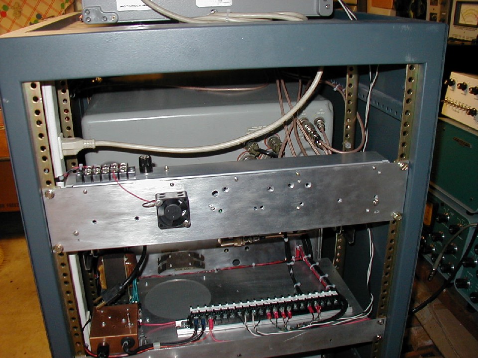
I built this in March 2007. With only two antennas and many receivers I needed to have some type of Multicoupler I could connect all the radios to so I didn't have to keep reaching behind radios and connecting/disconnecting antennas. I've had a copy of Phil Atchley's LF-HF Receiver Multicoupler for some time and decided it was time to build this Multicoupler. |
|
|
 |
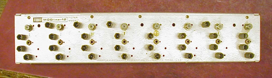
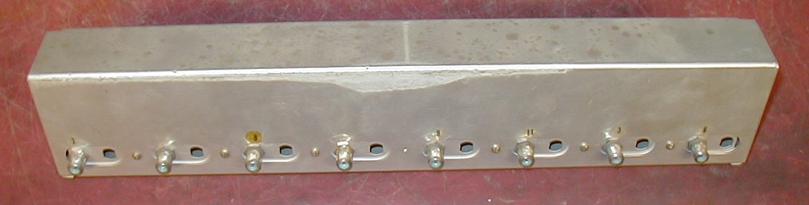
| First thing needed was to determine what to build this into. I had an old Jerrold Modline-12 TV Filter laying around that I was probably never going to use so I decided to build it into this chasses. |
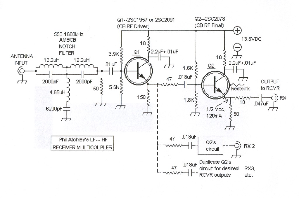
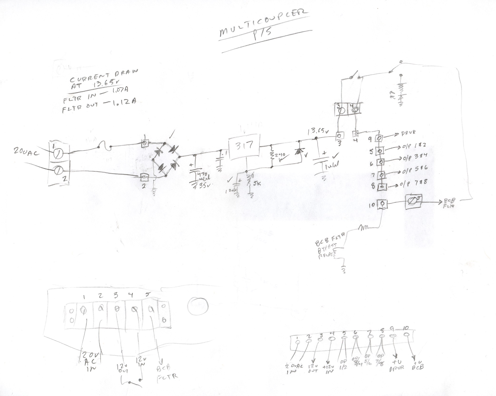
Here's the schematic of Phil's circuit he designed. I did some performance checks during and after this project and this design is an excellent Multicoupler design, well done Phil. I will present that data later. I have since learned that Steve AA7U and Phil collaborated together on the Multicoupler design. Steve did the original Paint diagram for Phil and also originally bread boarded the circuit and tested it on the bench for Phil, making some changes to arrive at the final circuit. great job by both of these guys. I decided to make 8 outputs and make the BCB filter in/out switch able. I also decided to modularize the construction so BCB filter would be a circuit board, input driver would be a separate ckt brd, each of the 8 outputs would be a separate ckt brd, and the power supply would be a separate ckt brd. |
 |
|
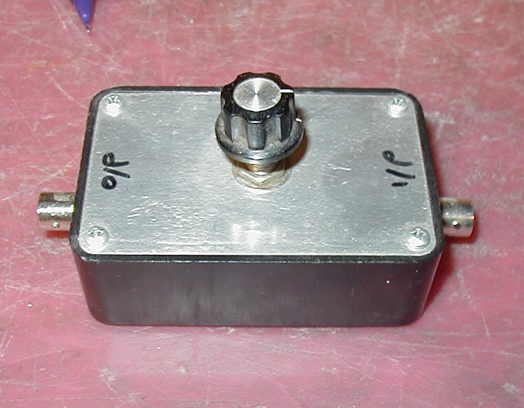
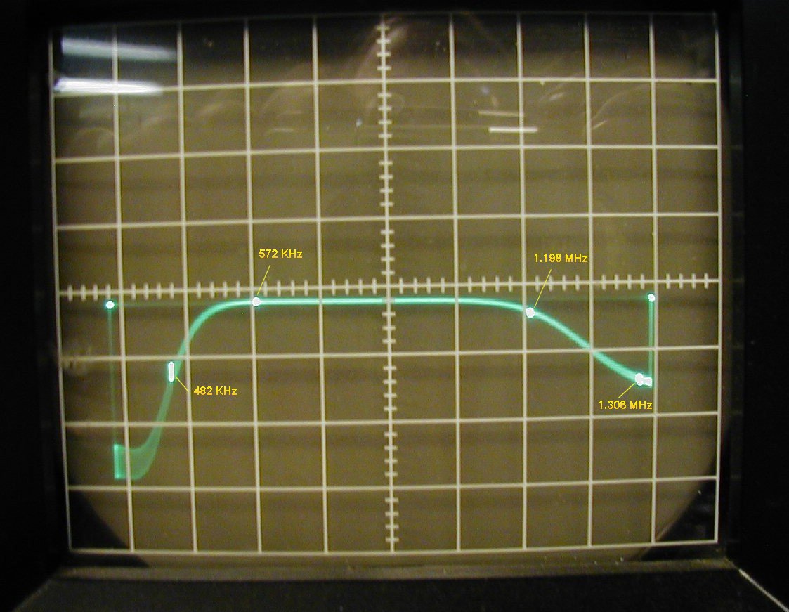
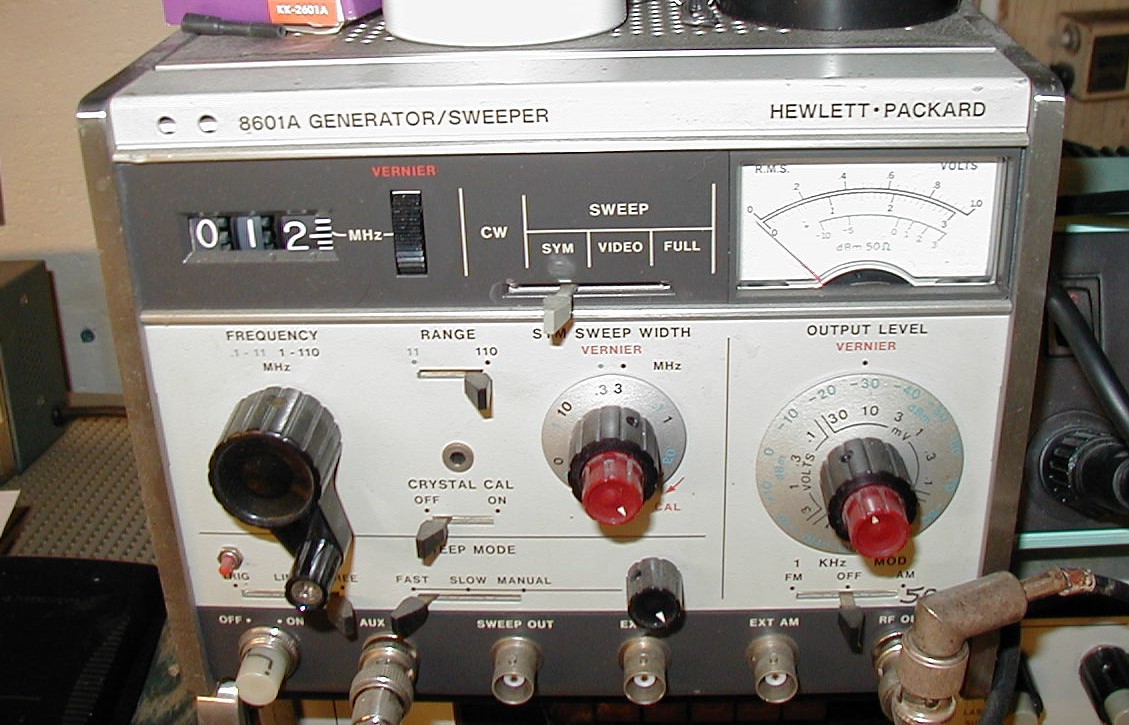
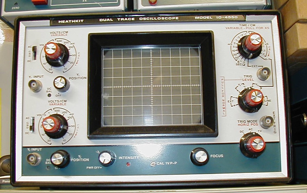
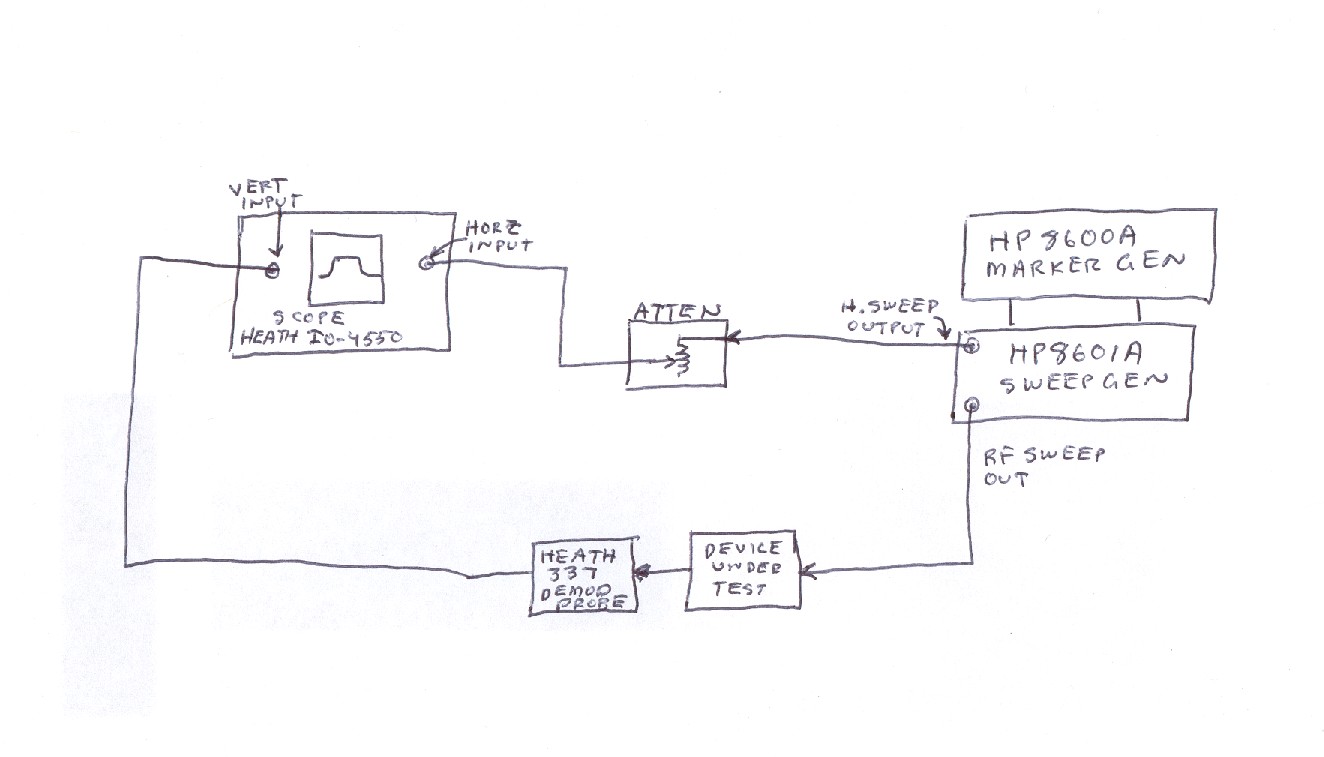
| I worked on the BCB Filter first. Before etching a board I wanted to check the performance of the BCB Filter so I bread boarded the filter and swept it. Above are the results, very impressive, great job again to Phil and this design. I have marked the frequencies for the markers shown in the trace. | Thought you might be interested in the test setup I used for sweeping. I used an HP8601A Sweep Gen, HP8600A Marker Gen, Heath 337 Demod Probe, Heath IO-4550 O'Scope and an attenuator I made because I needed to control the level of the sweep sawtooth to the Horz input to the scope. Above are the pieces. |
 |
 |
|
Here's the basic test setup. The Demod probe is a negative detector so it produces a negative output voltage proportional to signal level. In the waveform shown above you can see that the positive part of the waveform is actually the BCB attenuation, this is why the above waveform shows a positive going attenuation trace. |
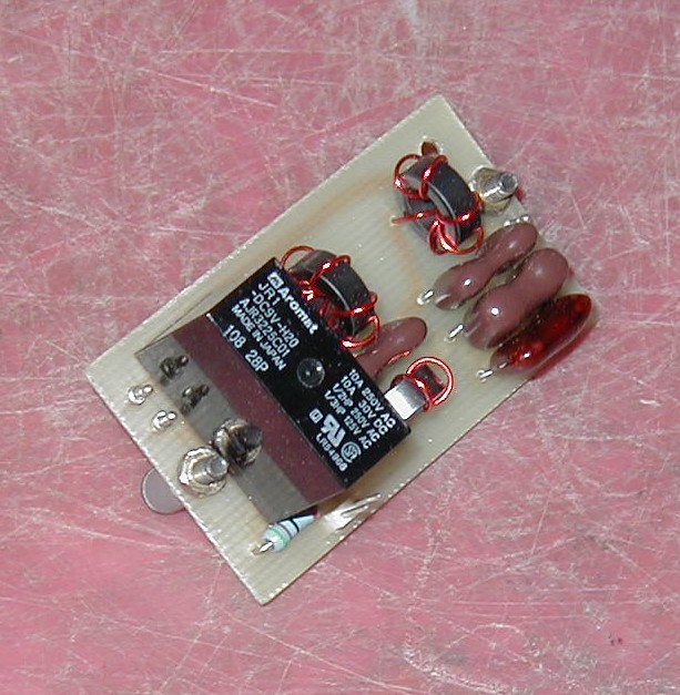
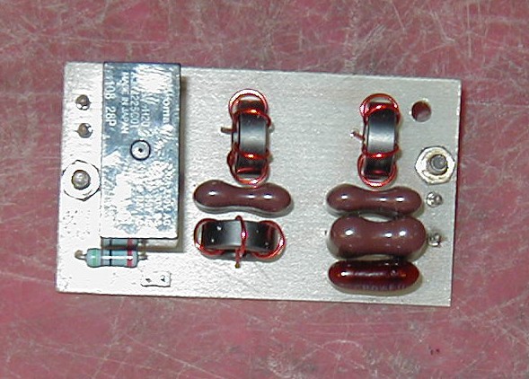
Here's a couple shots of the completed BCB Filter board. |
 |
 |
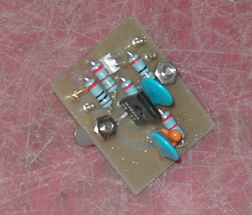
| Driver Brd was next. |
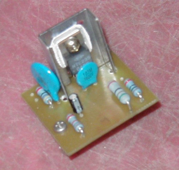
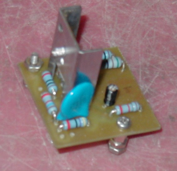
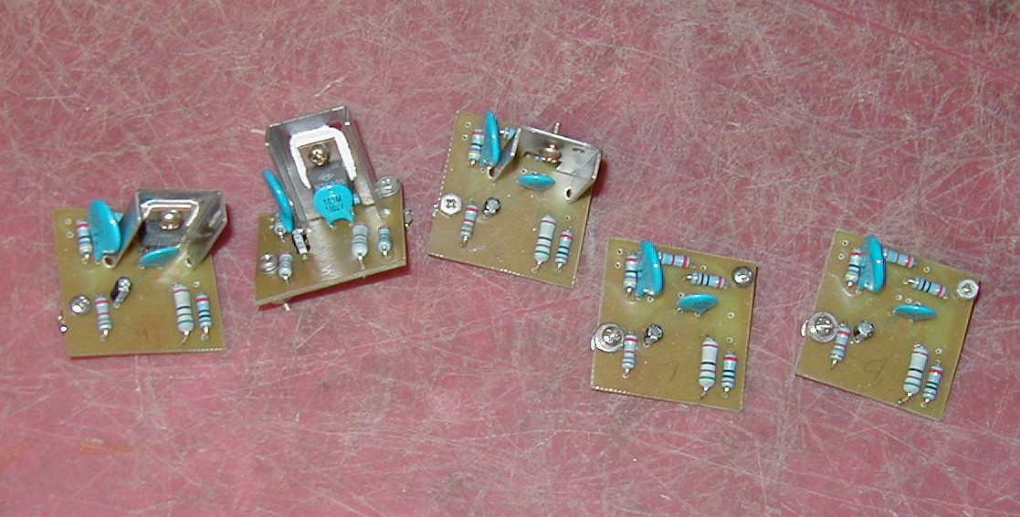
Next was the output boards. I made 8 of them. Above shown in various states of assembly. Heat sinks are definitely required and Phil specifies this in his design. The Outputs are emitter follower circuits that are biased so that half Vcc is on the emitter and you will have about 120ma of static current flow through the output transistor. So, with about 6.5 volts across the transistor and 120ma flowing through it P=EI says that statically the transistor will need to dissipate about 780mw. They do get warm so I would not chance going without the heat sinks. |
 |
.JPG)
.JPG) |
|
Next was the power supply. This schematic was the final cut. It's a basic 3 terminal regulator ckt. Learned a lot about designing power supplies using these 3 terminal devices. There are some gotcha's when working with them that you have to look out for. This is the scribble working version. |
Here's the first pass at the power supply. Couple things to note that will end up changing. The 3 terminal reg is mounted on the circuit board with no heat sink and I had a 12.6VAC transformer attached to the chassis for the power supply. My intent was to supply 115vac to the unit on the terminal board, this is going to change to. The pwr supply needed to produce 12vdc and supply a little over an amp of current. I figured I had plenty of head room with a 2amp capable transformer as there would be about 15vdc after full wave rectification and filtering. The device was guaranteed to provide 1.5 amps before internal current limiting. I only needed to flow a little over 1 amp so I should have plenty of head room, right? Wrong assumption! |
|
Here's what I learned: After initially assembling (and installing before bread boarding and testing, you'd think I would know better by now) the power supply worked fine with no load. But, as I started adding load things began to happen after about a half amp of load. Regulated voltage was dropping as I added load above a half amp. How could this be, this device is supposed to regulate at the desired setting and guaranteed 1.5 amp output. What was happening was that as load current was drawn, output voltage from the bridge (input to the device) was dropping. This was due to voltage being dropped across the internal resistance of the transformer secondary as current flow through it began to increase. This is normal power supply action, stuff you learn about in basic electronics. This is were I learned how critical voltage drop across the regulator is if you want to maintain a regulated output at rated, guaranteed, current flow (basic stuff again but it took this working example to make me again aware of the basics). Through testing and reading the spec sheet I determined that the optimal voltage drop across the device needed to be at a min of 3v. Higher voltage drops were okay, but had some considerations that needed looking at which I will talk about later. But, anything less than three volts across the device and things began to get unstable with the regulator. So I had several alternatives. 1) Get a 12.6vac transformer with a higher current rating which would have lower internal winding resistance and less voltage dropped across the internal resistance. 2) Put a bigger, mondo, filter cap at the output of the bridge which would maintain the bridge output voltage between rectification peaks, or 3) get a transformer with greater secondary voltage somewhere between 16 and 20vac. I went with number 3 and a little of number 2. I didn't want to put in a mondo filter cap and I didn't want to buy another transformer. I had a transformer on hand rated at 20vac at 4amps, this didn't cost anything so this is what I used and I did put in a slightly larger filter cap for good measure.
The regulator now worked properly regulating 12vdc all the way up to my required load of a little over an amp of current flow. But not for long! As I sat there beaming with pride I solved the problem, all of a sudden the voltage began to rapidly decrease. Turns out what I was seeing was the temp shutdown work perfectly as described in the specs. It was kind of cool to actually see the temp shutdown work, I now know it actually does work as spec'd. Here was my problem now. Yes, I was maintaining a voltage drop across the device of between 3-4 volts, and I was flowing about 1.2 amps through the device. Well if you do a little math, P=EI, 4volts time 1.2 amps = 4.8 watts! The device was dissipating almost 5 watts! Yes, it was getting HOT! Solution was to heatsink the device. I ended up doing this by taking the regulator off the board and mounting it to the chassis. This solved the problem.
Basic lessons learned: 1) Your gona need a transformer that produces an output that is 4-5 volts higher than your desired, regulated, output. A 12.6vac transformer will not work to produce a 12vdc output because you will not be able obtain enough difference across the regulating device. Of course this depends on how much current your gona draw. At lower currents it did work fine. But higher current draws will cause a problem with this close of values between transformer output and regulator output. 2) You need to be aware of the power the device will need to dissipate. Very simple calculation, voltage across the device times current through the device. The LM317 can regulate with voltage differences up to 40v across the device, but, you will need to heatsink. The greater the voltage drop across the device and the greater the current flow through the device will determine how much more heat sinking you will need. P=EI. 3) Don't skimp on the bridge filter cap. Use a big one, at least one as big as your project design will allow, you will have to make up for the rest in a greater value transformer output. |
.JPG)
.JPG)
 |
| Here's how the supply ended up. Note that the regulator was moved off the board and mounted to the chassis to heatsink it. Also, I installed a bigger filter cap off the board to help the situation. I still did get quite warm but was able to operate effectively and maintain a regulated output at 1.2 amps. I was still a little concerned because the box did still get quite warm. I mean not only was I dissipating the heat of the regulator but I was also dissipating heat in each one of the 8 output transistors and all that heat was bottled up inside that chassis. I was worried about cumulative heat over a period of time. I had run it 4 hours as a test and it did get very warm. I foresaw that this thing could be fired up for a week or more at a time. So I added a little 12vdc fan that can be seen in the third picture. It runs very cool now and I have piece of mind that its going to perform without worrying about it. One other note, I had to mount the transformer somewhere else because of it's size, I couldn't mount it on the Multicoupler chassis itself. You can see the transformer in the third picture on the shelf below the Multicoupler. The Multicoupler itself now requires a 20vac input at it's terminal board. |
.JPG)
.JPG) |
.JPG) |
|
Okay, back to building this thing. With all the boards made I started mounting them. Here's a couple shots of 3 of the 8 output boards. Installed. DC power to the boards is distributed by the stand off posts you see on the chassis. One stand off supplies the two boards on either side of the stand off. Input to the boards is the green wire hanging in the air in the pictures. Output from the boards capacitor couples directly from the board to the output BNC connector. |
Assembly moving along. BCB filter board mounted, input driver board mounted, and all the output boards mounted. Yes, that's the original power supply board. I did build the whole thing before I realized I had a power supply issue which just reinforces the breadboard and test methodology before building. Something along the lines of the measure twice cut once methodology. I should have know better, it's not like this is the first project I ever built. Anyway, at this point I was still waiting for the last three output transistors to come in, that's why you don't see heat sinks for the last three outputs. |
.JPG)
.JPG) |
.JPG) |
| Some more shots of it going together. Here you can see the input buss line for the output boards. It's the green wire coming from the driver board that fans out to standoffs by each output module. These stand offs are what the green wire from each of the output modules connect to. | Here it is, guts complete. Power supply revision and all. |
.JPG)
.JPG)
.JPG) |
| Here's some shots of it all closed up and ready to mount. Note I did not have the fan on it yet. That was another later revision I made after running it a while and not being comfortable with the cumulative heat build up in it. |
Performance
|
My method of test was to generate signal with an HP8640A which was input into the Multicoupler. Output was read using an HP141T Spectrum Analyzer. My input generated signal was at -40dBm in 1 MHz increments. Input and output were plotted in a table in Excel and then I made a chart out of the table data. If you have Excel click here and down load the entire spreadsheet data. Below are some summary charts. |
 |
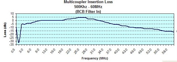 |
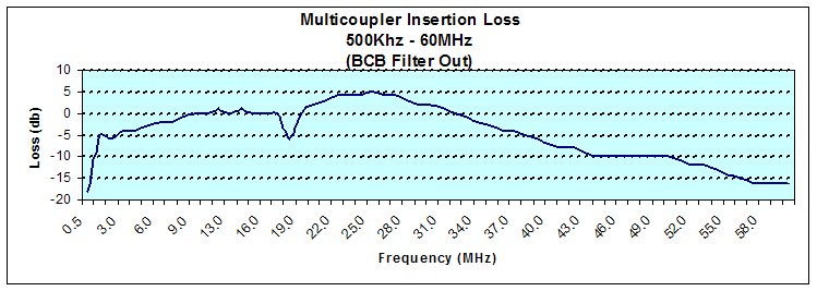
| This plot is a scan from 500KHz to 60MHz in 1 MHz increments with the BCB Filter switched out. Couple notes. Ideal would be a straight line across 0dB. Of course reality is otherwise. But this is actually pretty good. I'm satisfied with it. I'll get to that little notch at about 19MHz. | This plot is a scan from 500KHz to 60 MHz in 1 MHz increments again, but this time the BCB filter is switched in. Actually looks better with the BCB Filter in and note the notch around 19MHz is gone. Will get to that in a little bit. |
 |
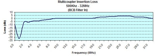 |
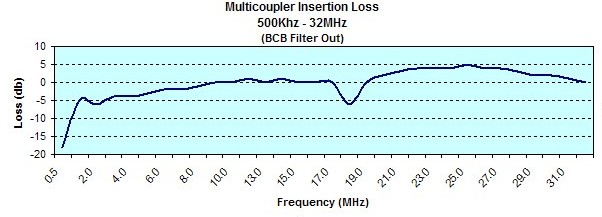
| This plot is more in line with the freq range it will be used in. This plot is a scan from 500KHz to 32 MHz in 1 MHz increments with the BCB filter switched out. Again, fairly flat, not bad, but there's that notch again at about 19 MHz. | This plot is again the scan from 500KHz to 32 MHz in 1 MHz increments again but this time with the BCB Filter switched in. Very nice response. Again, note that with the BCB Filter in the notch at 19 MHz is gone. One other note of interest in the above 4 plots. Note that the gain actually is in the plus dB's around 27 MHZ. The transistors used are spec'd as CB Radio driver and output transistors and it's very interesting that these plots actually show gain around 27MHz. Interesting. |
 |
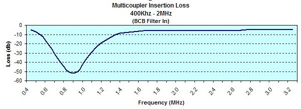 |
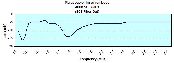
| Here's a narrowed down plot so we can get a better look at the filter response. This plot is from 500KHz to only 3.2 MHz in 100 KHz increments with the BCB Filter switched out. Note that there is a notch at about 1.4MHz which we couldn't see before but now shows up when we narrow down the scan width. Will get to this notch in a little bit. | Here's the 500KHz to 3.2 MHz plot in 100 KHz increments but with the BCB Filter now switched in. Note the very nice notch in the BCB area and the very nice almost flat response on the rest of the plot. Also note that the notch at 1.4 MHz is gone as well. Lets get to those notches. |
Those Notches
|
The notches are actually a design error on my part that I still need to fix. I know what is causing it and how to fix it just haven't done it yet. The problem was created because I was trying to cut corners bypassing the BCB Filter when it was switched out. |
 |
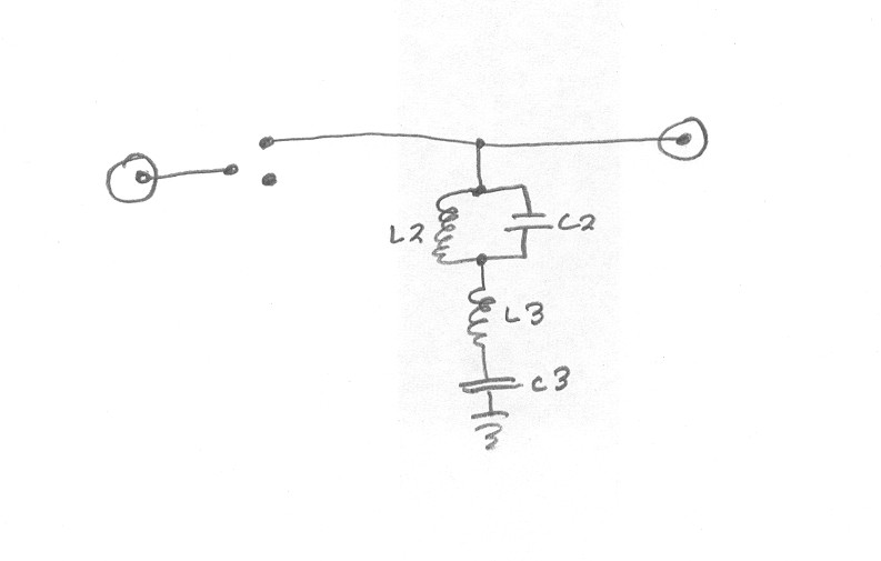 |
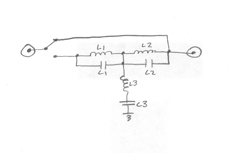
| Here's the BCB Filter and how I wired it to either switch it out or in. I wanted to only use one relay which I had on hand. There were several reasons for this, 1) relay I had was SPST, 2) I didn't want to use two relays as this meant more current draw from the power supply which was already at 1.2 amps and 3) this seemed like a ridiculously simple solution. Can you already see the flaw in the design. | Here's the problem. When the filter is switched out there is actually still reactive components left hanging on the input line. Above is the equivalent circuit when the BCB Filter is switched out. These reactive components still hanging on the line is what's causing the notches at 1.4 MHz and 19MHz. And it also explains why the notches go away when the filter is switched in. |
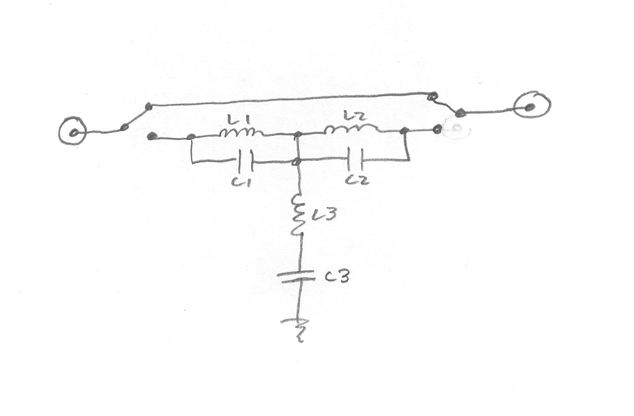 |
| Here's the solution. The filter needs to be completely bypassed on both sides, duh! And I thought I was being clever. This fix will require me to etch a new ckt brd. I will eventually get around to it but for now I am living with the notches, at least I'm aware they are there and I do know how to fix it. |